Integrated Photonic Component Design Series
Overview of the integrated photonic components I’ve been designing using GDSFactory, KLayout, and MEEP.
Over the past few weeks, I’ve been working on designing and modeling several integrated photonics components using tools like GDSFactory, KLayout, and MEEP. The goal is to create a complete library of fundamental photonic building blocks and study their optical performance through simulation.
This post serves as a summary and navigation page — linking to detailed posts for each component where I discuss the design process, parameters, and simulation results.
🧩 Passive Components
These are the basic on-chip elements for routing and manipulating light.
- Directional Coupler – Design and simulation of a compact Si directional coupler.
- Y-Branch Splitter – Power splitting using adiabatic Y-junctions.
- Ring Resonator – Resonant filtering and wavelength-selective behavior.
- Bragg Grating – Wavelength reflection and filtering with periodic structures.
- Mach–Zehnder Interferometer (MZI) – Phase-controlled interferometric filter (Circuit modeling using SAX).
💡 Optical I/O Components
Coupling light between the chip and the outside world.
- Grating Coupler – Vertical coupling of light using surface gratings.
- Edge Coupler – Efficient fiber-to-chip coupling at the facet.
⚙️ Active Components
These devices allow dynamic control of light using electrical, thermal, or phase-change mechanisms.
- Thermo-Optic MZI Phase Shifter – Tunable phase control using local heating.
- Ring Resonator Phase-Change Switch – Non-volatile optical switching using GST layers.
- PN Junction Modulator – Electro-optic modulation using carrier-depletion in a pn junction with TCAD simulation.
- Ring Modulator – Electro-optic modulation in ring resonator with TCAD simulation.
- [Photodetector] – On-chip detection using Ge or Si-based absorption.
Each of these components explores both device-level simulations (using MEEP) and compact modeling for system integration.
🔁 Photonic Circuit Modeling
At the circuit level, I use SAX and GDSFactory’s netlist tools to assemble and simulate multi-component photonic circuits.
⭐ Featured: CWDM using Cascaded MZI
A coarse wavelength division multiplexer designed using cascaded Mach-Zehnder interferometers for multi-channel wavelength separation. This flagship project showcases:
- 🔬 Complete modeling pipeline: FDTD characterization (MEEP) → Circuit assembly (SAX)
- 🎯 FSR engineering for precise channel spacing
- 🏗️ Hierarchical design from individual MZI blocks to full system integration
- 📡 Real-world WDM communication system demonstration
- MZI Circuit Simulation – Example of a interferometric system modeled using SAX.
Thermo-Optic MZI Phase Shifter – Tunable phase control using local heating using SAX.
- [Ring Filter Bank] – Modeling cascaded ring resonators and spectral responses.
- [Reconfigurable Switch Matrix] – Demonstration of signal routing using phase shifters and Y-branches.
The focus is on hierarchical circuit design, port-based modeling, and integration of measured or simulated S-parameters for realistic performance prediction.
🧬 Inverse Design & Topology Optimization
To push performance beyond conventional geometries, I’ve been exploring inverse design techniques using topology optimization.
- Optimized 1×2 MMI Splitter – Compact splitter designed via gradient-based inverse optimization for equal power splitting and phase control.
- [Inverse-Designed Grating Coupler] – A grating structure optimized using adjoint-based topology optimization to maximize coupling efficiency between a fiber mode and on-chip waveguide.
These designs employ adjoint sensitivity analysis to efficiently compute gradients with respect to material distribution, enabling automated discovery of non-intuitive geometries that outperform traditional hand-designed structures.
🧱 Modeling and Tools
All designs are implemented and simulated using:
- GDSFactory for layout generation and parameterized cell (PCell) design
- KLayout for GDS visualization and verification
- MEEP / MPB for FDTD and mode simulations
- Python for automated parameter sweeps and post-processing
- SAX for circuit modeling
Stay tuned — I’ll be publishing detailed writeups for each of these components, including:
- Layout generation code (
.py/.gds) - Optical mode and field distribution plots
- Transmission spectra and coupling efficiency
- Optimization steps
You can follow the Photonics Project Series to see all related posts as they’re added.
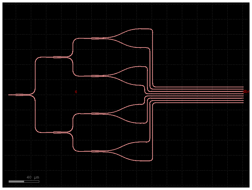
Code for the title circuit image
1
2
3
4
5
6
7
8
9
10
11
12
13
14
15
16
17
18
19
20
21
22
23
24
25
26
27
28
29
import gdsfactory as gf
import gdsfactory.schematic as gt
import yaml

n = 2**3
splitter = gf.components.splitter_tree(noutputs=n, spacing=(50, 50))
dbr_array = gf.components.array(
    component=gf.c.dbr, rows=n, columns=1, column_pitch=0, row_pitch=3, centered=True
)
s = gt.Schematic()
s.add_instance("s", gt.Instance(component=splitter))
s.add_instance("dbr", gt.Instance(component=dbr_array))
s.add_placement("s", gt.Placement(x=0, y=0))
s.add_placement("dbr", gt.Placement(x=300, y=0))

for i in range(n):
    s.add_net(
        gt.Net(
            p1=f"s,o2_2_{i+1}",
            p2=f"dbr,o1_{i+1}_1",
            name="splitter_to_dbr",
            settings=dict(radius=5, sort_ports=True, cross_section="strip"),
        )
    )

conf = s.netlist.model_dump(exclude_none=True)
yaml_component = yaml.safe_dump(conf)
circuit = gf.read.from_yaml(yaml_component)
circuit.plot()