Ring Modulator - PN Junction
Ring modulator PN Junction
Source Code
1
2
3
4
5
6
7
8
9
10
11
12
13
14
15
16
17
18
19
20
21
22
# Import the necassry packages
import gplugins.modes as gm
import gplugins.gmeep as gmeep
import numpy as np
import matplotlib.pyplot as plt
import matplotlib.patches as patches
import meep as mp
import gplugins.tidy3d as gt
import gdsfactory as gf
# from ubcpdk import PDK, cells
from functools import partial
# PDK.activate()
import sax
from jax import config
config.update("jax_enable_x64", True)
import jax
import jax.numpy as jnp
from simphony.libraries import siepic
from gplugins.devsim import get_simulation_xsection
from gplugins.devsim.get_simulation_xsection import k_to_alpha, clear_devsim_cache
import pyvista as pv
import os
1
2
3
4
5
6
7
8
Using MPI version 4.1, 1 processes
[32m2025-12-10 01:53:50.527[0m | [1mINFO [0m | [36mgplugins.gmeep[0m:[36m<module>[0m:[36m39[0m - [1mMeep '1.31.0' installed at ['/home/ramprakash/anaconda3/envs/si_photo/lib/python3.13/site-packages/meep'][0m
Searching DEVSIM_MATH_LIBS="libopenblas.so:liblapack.so:libblas.so"
Loading "libopenblas.so": ALL BLAS/LAPACK LOADED
Skipping liblapack.so
Skipping libblas.so
loading UMFPACK 5.1 as direct solver
[32m2025-12-10 01:53:53.389[0m | [1mINFO [0m | [36mgplugins.devsim[0m:[36m<module>[0m:[36m16[0m - [1mDEVSIM '2.10.0' installed at ['/home/ramprakash/anaconda3/envs/si_photo/lib/python3.13/site-packages/devsim'][0m
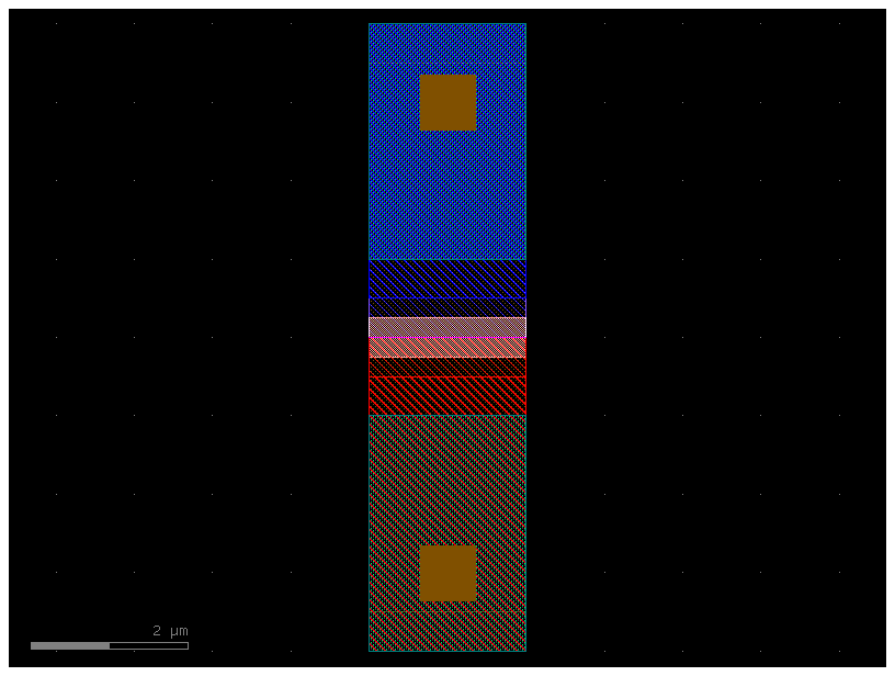
Design of PN junction
Loading a straing pn junciton component from gdsfactory
The aim is to do full TCAD simulation to get the Vpi
Step 1: Import PN junction straight waveguide form GDSFactory
Source Code
1
2
3
4
5
6
7
8
9
10
11
12
13
14
15
16
17
import gdsfactory as gf
from gdsfactory.generic_tech import LAYER, LAYER_STACK
from gdsfactory.technology import LayerLevel, LayerStack

# We choose a representative subdomain of the component
waveguide = gf.Component()
waveguide.add_ref(
    gf.functions.trim(
        component=gf.components.straight_pn(length=10, taper=None).copy(),
        domain=[[3, -4], [3, 4], [5, 4], [5, -4]],
    )
)

waveguide.plot()

scene = waveguide.to_3d()
scene.show()
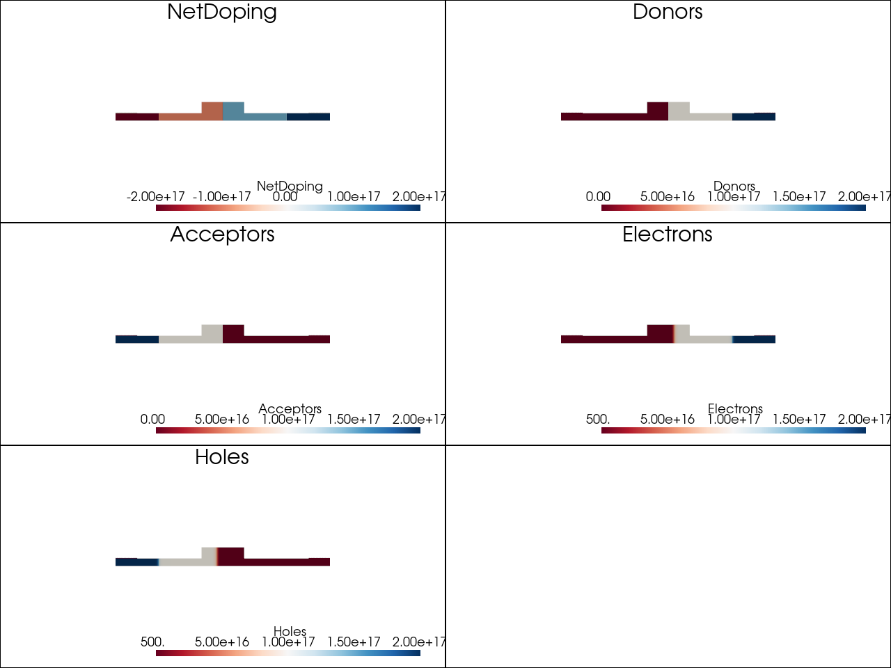
Run a TCAD simualtion to calculate the carrier desnity of electron (dN) and holes (dP)
Source Code
1
2
3
active_layer_stack = gf.pdk.get_active_pdk().layer_stack
active_layer_stack.layers
1
2
3
4
5
6
7
8
9
10
11
12
13
14
15
16
17
18
{'substrate': LayerLevel(name=None, layer=WAFER, derived_layer=None, thickness=10.0, thickness_tolerance=None, width_tolerance=None, zmin=-13.0, zmin_tolerance=None, sidewall_angle=0.0, sidewall_angle_tolerance=None, width_to_z=0.0, z_to_bias=None, bias=None, mesh_order=101, material='si', info={}),
 'box': LayerLevel(name=None, layer=WAFER, derived_layer=None, thickness=3.0, thickness_tolerance=None, width_tolerance=None, zmin=-3.0, zmin_tolerance=None, sidewall_angle=0.0, sidewall_angle_tolerance=None, width_to_z=0.0, z_to_bias=None, bias=None, mesh_order=9, material='sio2', info={}),
 'core': LayerLevel(name=None, layer=((WG - DEEP_ETCH) - SHALLOW_ETCH), derived_layer=WG, thickness=0.22, thickness_tolerance=None, width_tolerance=None, zmin=0.0, zmin_tolerance=None, sidewall_angle=10.0, sidewall_angle_tolerance=None, width_to_z=0.5, z_to_bias=None, bias=None, mesh_order=2, material='si', info={}),
 'shallow_etch': LayerLevel(name=None, layer=(SHALLOW_ETCH & WG), derived_layer=SLAB150, thickness=0.07, thickness_tolerance=None, width_tolerance=None, zmin=0.0, zmin_tolerance=None, sidewall_angle=0.0, sidewall_angle_tolerance=None, width_to_z=0.0, z_to_bias=None, bias=None, mesh_order=1, material='si', info={}),
 'deep_etch': LayerLevel(name=None, layer=DEEP_ETCH, derived_layer=SLAB90, thickness=0.13, thickness_tolerance=None, width_tolerance=None, zmin=0.0, zmin_tolerance=None, sidewall_angle=0.0, sidewall_angle_tolerance=None, width_to_z=0.0, z_to_bias=None, bias=None, mesh_order=1, material='si', info={}),
 'clad': LayerLevel(name=None, layer=WAFER, derived_layer=None, thickness=3.0, thickness_tolerance=None, width_tolerance=None, zmin=0.0, zmin_tolerance=None, sidewall_angle=0.0, sidewall_angle_tolerance=None, width_to_z=0.0, z_to_bias=None, bias=None, mesh_order=10, material='sio2', info={}),
 'slab150': LayerLevel(name=None, layer=SLAB150, derived_layer=None, thickness=0.15, thickness_tolerance=None, width_tolerance=None, zmin=0.0, zmin_tolerance=None, sidewall_angle=0.0, sidewall_angle_tolerance=None, width_to_z=0.0, z_to_bias=None, bias=None, mesh_order=3, material='si', info={}),
 'slab90': LayerLevel(name=None, layer=SLAB90, derived_layer=None, thickness=0.09, thickness_tolerance=None, width_tolerance=None, zmin=0.0, zmin_tolerance=None, sidewall_angle=0.0, sidewall_angle_tolerance=None, width_to_z=0.0, z_to_bias=None, bias=None, mesh_order=2, material='si', info={}),
 'nitride': LayerLevel(name=None, layer=WGN, derived_layer=None, thickness=0.35000000000000003, thickness_tolerance=None, width_tolerance=None, zmin=0.32, zmin_tolerance=None, sidewall_angle=0.0, sidewall_angle_tolerance=None, width_to_z=0.0, z_to_bias=None, bias=None, mesh_order=2, material='sin', info={}),
 'ge': LayerLevel(name=None, layer=GE, derived_layer=None, thickness=0.5, thickness_tolerance=None, width_tolerance=None, zmin=0.22, zmin_tolerance=None, sidewall_angle=0.0, sidewall_angle_tolerance=None, width_to_z=0.0, z_to_bias=None, bias=None, mesh_order=1, material='ge', info={}),
 'undercut': LayerLevel(name=None, layer=UNDERCUT, derived_layer=None, thickness=-5.0, thickness_tolerance=None, width_tolerance=None, zmin=-3.0, zmin_tolerance=None, sidewall_angle=0.0, sidewall_angle_tolerance=None, width_to_z=0.0, z_to_bias=([0.0, 0.3, 0.6, 0.8, 0.9, 1.0], [0.0, -0.5, -1.0, -1.5, -2.0, -2.5]), bias=None, mesh_order=1, material='air', info={}),
 'via_contact': LayerLevel(name=None, layer=VIAC, derived_layer=None, thickness=1.01, thickness_tolerance=None, width_tolerance=None, zmin=0.09, zmin_tolerance=None, sidewall_angle=-10.0, sidewall_angle_tolerance=None, width_to_z=0.0, z_to_bias=None, bias=None, mesh_order=1, material='Aluminum', info={}),
 'metal1': LayerLevel(name=None, layer=M1, derived_layer=None, thickness=0.7000000000000001, thickness_tolerance=None, width_tolerance=None, zmin=1.1, zmin_tolerance=None, sidewall_angle=0.0, sidewall_angle_tolerance=None, width_to_z=0.0, z_to_bias=None, bias=None, mesh_order=2, material='Aluminum', info={}),
 'heater': LayerLevel(name=None, layer=HEATER, derived_layer=None, thickness=0.75, thickness_tolerance=None, width_tolerance=None, zmin=1.1, zmin_tolerance=None, sidewall_angle=0.0, sidewall_angle_tolerance=None, width_to_z=0.0, z_to_bias=None, bias=None, mesh_order=2, material='TiN', info={}),
 'via1': LayerLevel(name=None, layer=VIA1, derived_layer=None, thickness=0.49999999999999956, thickness_tolerance=None, width_tolerance=None, zmin=1.8000000000000003, zmin_tolerance=None, sidewall_angle=0.0, sidewall_angle_tolerance=None, width_to_z=0.0, z_to_bias=None, bias=None, mesh_order=1, material='Aluminum', info={}),
 'metal2': LayerLevel(name=None, layer=M2, derived_layer=None, thickness=0.7000000000000001, thickness_tolerance=None, width_tolerance=None, zmin=2.3, zmin_tolerance=None, sidewall_angle=0.0, sidewall_angle_tolerance=None, width_to_z=0.0, z_to_bias=None, bias=None, mesh_order=2, material='Aluminum', info={}),
 'via2': LayerLevel(name=None, layer=VIA2, derived_layer=None, thickness=0.20000000000000018, thickness_tolerance=None, width_tolerance=None, zmin=3.0, zmin_tolerance=None, sidewall_angle=0.0, sidewall_angle_tolerance=None, width_to_z=0.0, z_to_bias=None, bias=None, mesh_order=1, material='Aluminum', info={}),
 'metal3': LayerLevel(name=None, layer=M3, derived_layer=None, thickness=2.0, thickness_tolerance=None, width_tolerance=None, zmin=3.2, zmin_tolerance=None, sidewall_angle=0.0, sidewall_angle_tolerance=None, width_to_z=0.0, z_to_bias=None, bias=None, mesh_order=2, material='Aluminum', info={})}
Simple step doping. See below for complex doping profile
Source Code
1
2
3
4
5
6
7
8
9
10
11
12
%%capture
um = 1e-6
c = get_simulation_xsection.PINWaveguide(
    core_width=0.500 * um,
    core_thickness=0.220 * um,
    slab_thickness=0.090 * um,
)
# Initialize mesh and solver
clear_devsim_cache()
c.ddsolver()
c.save_device('straight_PN.dat')
Source Code
1
2
3
4
5
6
7
8
9
10
11
12
13
14
15
16
17
18
19
20
21
22
23
24
25
26
27
28
29
30
31
mesh = pv.read('straight_PN.dat')
fields = [
    "NetDoping","Donors","Acceptors",
    "Electrons","Holes"]

p = pv.Plotter(shape=(3,2), notebook='static', window_size=(320*4, 240*4))
# c.plot(scalars="NetDoping", jupyter_backend="static")

idx = 0
for r in range(3):
    for ccol in range(2):
        p.subplot(r, ccol)

        if idx >= len(fields):
            p.add_text("")  # empty cell
            continue

        fname = fields[idx]
        idx += 1

        # if fname not in mesh.array_names:
        #     p.add_text(f"Missing {fname}")
        #     continue

        p.add_mesh(mesh, scalars=fname, cmap="RdBu")
        p.add_text(fname, position="upper_edge", font_size=12)
        _ = p.camera_position = "xy"
        p.add_scalar_bar(title=fname)

p.link_views()
p.show()
1
2
3
4
5
6
7
[0m[33m2025-12-09 13:17:00.350 ( 114.370s) [ 766F7929F740]vtkXOpenGLRenderWindow.:1458 WARN| bad X server connection. DISPLAY=[0m
/home/ramprakash/anaconda3/envs/si_photo/lib/python3.13/site-packages/pyvista/jupyter/notebook.py:56: UserWarning: Failed to use notebook backend:
No module named 'trame'
Falling back to a static output.
warnings.warn(
Applying voltage and finding the solution
Making waveguide from the devsim device with perturebd index and calculaitng the effective index. Using tidy3d for the mode calcaultions
Source Code
1
2
3
4
5
6
7
8
9
10
11
12
13
14
15
16
17
18
19
20
21
22
23
%%capture
voltages = [0, -0.5, -1, -1.5, -2, -2.5, -3, -3.5, -4, -5, -6, -7, -8, -9, -10]
ramp_rate = -0.1

n_dist = {}
neffs = {}
clear_devsim_cache()
um = 1e-6

dev = get_simulation_xsection.PINWaveguide(
    core_width=0.500 * um,
    core_thickness=0.220 * um,
    slab_thickness=0.090 * um,
)
dev.ddsolver()     # fresh, clean equilibrium state
for ind, voltage in enumerate(voltages):
    Vinit = 0 if ind == 0 else voltages[ind - 1]
    dev.ramp_voltage(Vfinal=voltage, Vstep=ramp_rate, Vinit=Vinit)
    waveguide = dev.make_waveguide(wavelength=1.55,grid_resolution=20)
    n_dist[voltage] = waveguide.index.values
    neffs[voltage] = waveguide.n_eff[0]

np.save("neffs_TCAD.npz", neffs)
Source Code
1
2
3
4
5
6
7
8
9
10
11
12
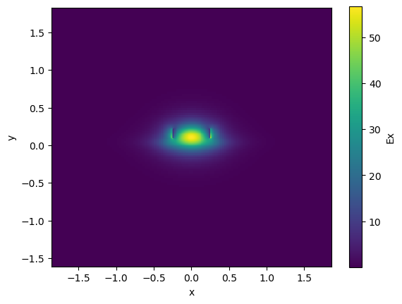
import gplugins.tidy3d as td
wg_td = td.modes.Waveguide(wavelength=1.55,
core_width=0.5,
core_thickness=0.22,
slab_thickness=0.090,
grid_resolution=50,
core_material='si',
clad_material='sio2',
cache_path=None,
overwrite=True)
wg_td.plot_field('Ex')
wg_td.n_eff[0]
1
np.complex128(2.5932203425309455+3.8757826065200905e-05j)
Source Code
1
2
3
4
5
6
7
8
9
10
11
12
13
14
15
16
17
neffs = {0: np.complex128(2.579233149832461+4.2558454254802517e-05j),
 -0.5: np.complex128(2.579248605051533+4.20043472854569e-05j),
 -1: np.complex128(2.5792605310824923+4.1578101252069765e-05j),
 -1.5: np.complex128(2.5792684479189205+4.1298845722944675e-05j),
 -2: np.complex128(2.5792768911186554+4.100265496131908e-05j),
 -2.5: np.complex128(2.579284107736812+4.0752849952389265e-05j),
 -3: np.complex128(2.5719153080505834+4.2195904369172816e-05j),
 -3.5: np.complex128(2.5792960309736594+4.033633789155556e-05j),
 -4: np.complex128(2.57930195707953+4.012628342291738e-05j),
 -5: np.complex128(2.5793103370214245+3.9827958190374006e-05j),
 -6: np.complex128(2.5793178726112416+3.956270654250005e-05j),
 -7: np.complex128(2.579323275257858+3.935982457145146e-05j),
 -8: np.complex128(2.5719524331528962+4.084224984011639e-05j),
 -9: np.complex128(2.5793333855608185+3.901735265199731e-05j),
 -10: np.complex128(2.5793378293861204+3.888440364347489e-05j)}

neffs
1
2
3
4
5
6
7
8
9
10
11
12
13
14
15
{0: np.complex128(2.579233149832461+4.2558454254802517e-05j),
 -0.5: np.complex128(2.579248605051533+4.20043472854569e-05j),
 -1: np.complex128(2.5792605310824923+4.1578101252069765e-05j),
 -1.5: np.complex128(2.5792684479189205+4.1298845722944675e-05j),
 -2: np.complex128(2.5792768911186554+4.100265496131908e-05j),
 -2.5: np.complex128(2.579284107736812+4.0752849952389265e-05j),
 -3: np.complex128(2.5719153080505834+4.2195904369172816e-05j),
 -3.5: np.complex128(2.5792960309736594+4.033633789155556e-05j),
 -4: np.complex128(2.57930195707953+4.012628342291738e-05j),
 -5: np.complex128(2.5793103370214245+3.9827958190374006e-05j),
 -6: np.complex128(2.5793178726112416+3.956270654250005e-05j),
 -7: np.complex128(2.579323275257858+3.935982457145146e-05j),
 -8: np.complex128(2.5719524331528962+4.084224984011639e-05j),
 -9: np.complex128(2.5793333855608185+3.901735265199731e-05j),
 -10: np.complex128(2.5793378293861204+3.888440364347489e-05j)}
Source Code
1
2
3
4
5
6
7
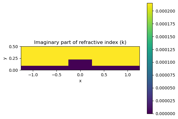
c_undoped = c.make_waveguide(wavelength=1.55, perturb=False, precision="double", grid_resolution=20)
# c_undoped.compute_modes()
n_undoped = c_undoped.index.values
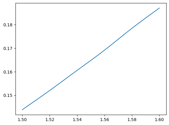
ax2 = c_undoped.index.imag.plot()
ax2.axes.set_aspect("equal")
ax2.axes.set_ylim([0, 0.5])
plt.title("Imaginary part of refractive index (k)")
1
Text(0.5, 1.0, 'Imaginary part of refractive index (k)')
Source Code
1
2
3
4
5
6
7
8
9
10
11
12
13
14
15
16
17
18
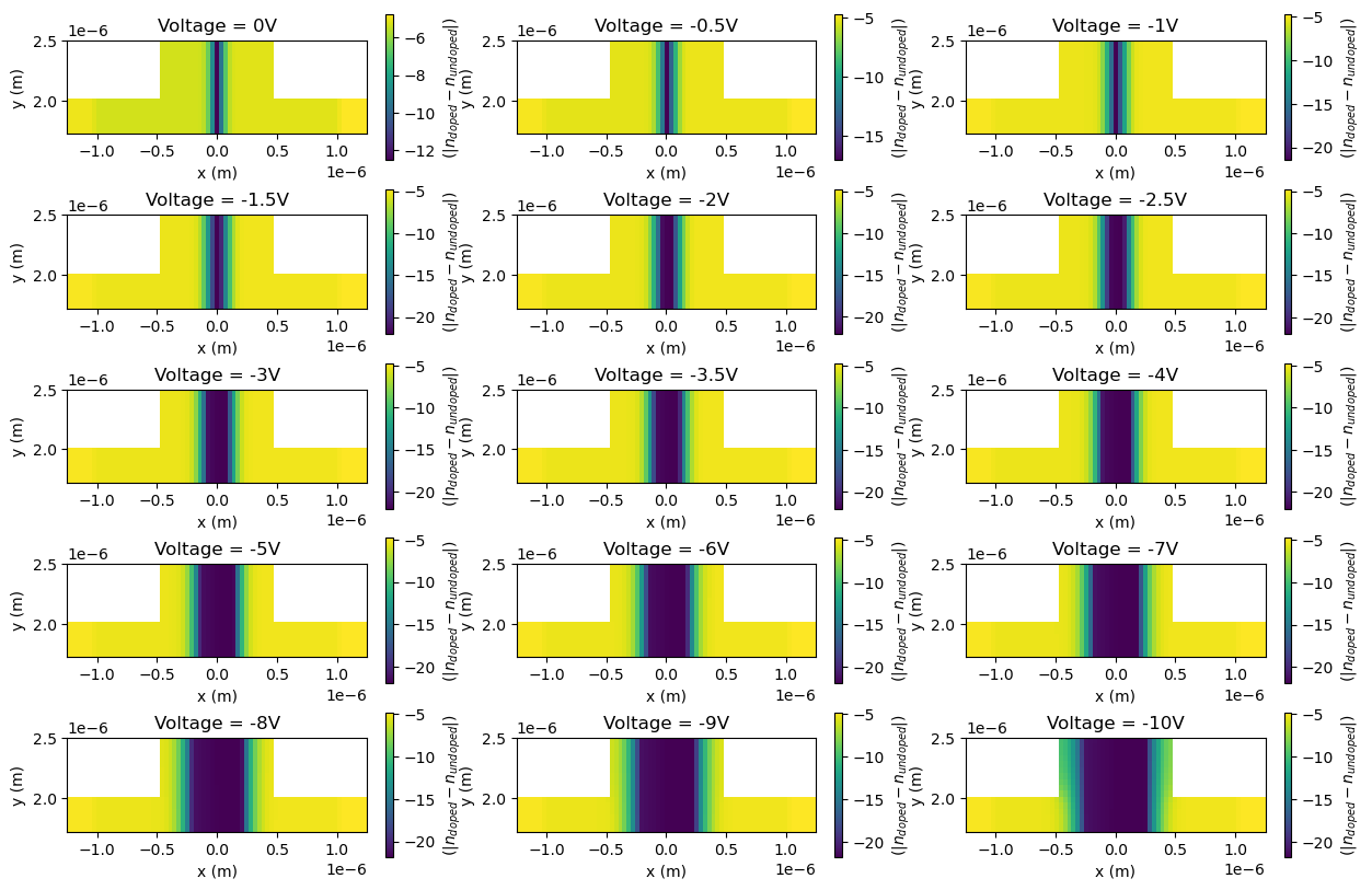
plt.figure(figsize=(15,10))
for ind, voltage in enumerate(voltages):
plt.subplot(5,3,ind+1)
plt.imshow(
np.log10(np.abs(np.imag(n_dist[voltage]- n_undoped))),
origin="lower",
extent=[
-c.xmargin - c.ppp_offset - c.core_width / 2,
c.xmargin + c.npp_offset + c.core_width / 2,
0,
c.clad_thickness + c.box_thickness + c.core_thickness,
],
)
plt.colorbar(label="$(|n_{doped} - n_{undoped}|)$")
plt.xlabel("x (m)")
plt.ylabel("y (m)")
plt.ylim(1.72e-6, 2.5e-6)
plt.title(f"Voltage = {voltage}V")
1
2
/tmp/ipykernel_2576937/1825642260.py:5: RuntimeWarning: divide by zero encountered in log10
  np.log10(np.abs(np.imag(n_dist[voltage]- n_undoped))),
Calacute the Vpi then have to build the compact model for the same. Finally use this in the ring resonator model
Phase change can be claculated form dn. So using this Vpi is calcaulted
Not too good - But okay for a proof of concept design
Calcaultion of $\Delta\phi$, $V_\pi$, and losses
Source Code
1
2
3
4
5
6
7
8
9
10
11
12
13
14
15
16
17
18
19
20
21
22
23
24
25
26
27
28
29
30
31
32
33
34
35
36
37
38
39
40
41
42
43
44
45
46
47
48
49
50
51
52
53
54
55
56
57
58
59
60
61
62
63
64
65
66
67
68
69
70
71
72
73
74
75
76
77
78
79
80
81
82
83
84
85
86
87
88
89
90
91
92
93
94
95
96
97
98
99
100
101
102
103
104
105
106
107
108
109
110
111
112
113
114
115
116
117
118
119
120
121
122
123
124
125
126
127
128
129
130
131
132
133
134
135
136
137
138
139
140
141
142
143
144
145
146
147
148
149
150
151
152
153
from scipy.interpolate import interp1d

# ============================================
# Step 1: Load TCAD data and fit polynomials
# ============================================
neffs = np.load("neffs_TCAD.npy", allow_pickle=True)
neffs_data = neffs[()]
voltages_data = np.array(sorted(neffs_data.keys()))
neff_values = np.array([neffs_data[v] for v in voltages_data])
neff_real_data = np.real(neff_values)
neff_imag_data = np.imag(neff_values)

# Create interpolation functions (cubic spline for smoothness)
neff_real_interp = interp1d(voltages_data, neff_real_data, kind='cubic',
                            fill_value='extrapolate', bounds_error=False)
neff_imag_interp = interp1d(voltages_data, neff_imag_data, kind='cubic',
                            fill_value='extrapolate', bounds_error=False)

# Fit polynomials for JAX compatibility
poly_real_coeffs = np.polyfit(voltages_data, neff_real_data, deg=4)
poly_imag_coeffs = np.polyfit(voltages_data, neff_imag_data, deg=4)

# Convert to JAX arrays
poly_real_coeffs_jax = jnp.array(poly_real_coeffs)
poly_imag_coeffs_jax = jnp.array(poly_imag_coeffs)

# Reference values at V=0
neff0_real = float(neff_real_interp(0.0))
neff0_imag = float(neff_imag_interp(0.0))

print(f"Reference neff at V=0: {neff0_real:.6f} + {neff0_imag:.6e}j")
print(f"Polynomial coefficients (real): {poly_real_coeffs}")
print(f"Polynomial coefficients (imag): {poly_imag_coeffs}")

# ============================================
# Step 3: Validation and Visualization
# ============================================

def validate_pn_model():
    """Validate the PN junction model against TCAD data"""

    V_test = np.linspace(0, -10, 100)

    # Calculate delta phase and loss changes
    delta_phases = []
    delta_losses = []

    for v in V_test:
        neff_real_V = np.polyval(poly_real_coeffs, v)
        neff_imag_V = np.polyval(poly_imag_coeffs, v)
        delta_neff_real = neff_real_V - neff0_real
        delta_neff_imag = neff_imag_V - neff0_imag

        # Delta phase for 100 μm
        delta_phi = 2 * np.pi * delta_neff_real * 100.0 / 1.55
        delta_phases.append(delta_phi)

        # Delta loss for 100 μm (CORRECTED)
        wl_cm = 1.55 * 1e-4
        length_cm = 100.0 * 1e-4
        delta_loss_per_cm = (4 * np.pi * delta_neff_imag * 4.343) / wl_cm
        delta_loss = delta_loss_per_cm * length_cm
        delta_losses.append(delta_loss)

    delta_phases = np.array(delta_phases)
    delta_losses = np.array(delta_losses)

    # Plot
    fig, axes = plt.subplots(2, 2, figsize=(14, 10))

    # Plot 1: Real(neff)
    axes[0, 0].plot(voltages_data, neff_real_data, 'o', markersize=8, label='TCAD data')
    V_fine = np.linspace(0, -10, 200)
    neff_real_fit = np.polyval(poly_real_coeffs, V_fine)
    axes[0, 0].plot(V_fine, neff_real_fit, '-', linewidth=2, label='Polynomial fit')
    axes[0, 0].set_xlabel('Voltage (V)', fontsize=12)
    axes[0, 0].set_ylabel('Real(n$_{eff}$)', fontsize=12)
    axes[0, 0].legend()
    axes[0, 0].grid(True, alpha=0.3)
    axes[0, 0].set_title('Effective Index (Real Part)')

    # Plot 2: Imag(neff)
    axes[0, 1].plot(voltages_data, neff_imag_data * 1e5, 'o', markersize=8, label='TCAD data')
    neff_imag_fit = np.polyval(poly_imag_coeffs, V_fine)
    axes[0, 1].plot(V_fine, neff_imag_fit * 1e5, '-', linewidth=2, label='Polynomial fit')
    axes[0, 1].set_xlabel('Voltage (V)', fontsize=12)
    axes[0, 1].set_ylabel('Imag(n$_{eff}$) × 10$^5$', fontsize=12)
    axes[0, 1].legend()
    axes[0, 1].grid(True, alpha=0.3)
    axes[0, 1].set_title('Effective Index (Imaginary Part)')

    # Plot 3: DELTA Phase (CORRECTED)
    delta_phases_per_cm = delta_phases / (100e-4)
    axes[1, 0].plot(-V_test, delta_phases_per_cm / np.pi, '-', linewidth=2)
    axes[1, 0].axhline(y=1, color='r', linestyle='--', linewidth=2, label='π phase shift')
    axes[1, 0].set_xlabel('Voltage (Reverse bias) [V]', fontsize=12)
    axes[1, 0].set_ylabel('Δφ (π rad/cm)', fontsize=12)
    axes[1, 0].legend()
    axes[1, 0].grid(True, alpha=0.3)
    axes[1, 0].set_title('Delta Phase Shift vs Voltage (from V=0)')

    # Plot 4: DELTA Loss (CORRECTED)
    delta_losses_per_cm = delta_losses / (100e-4)
    axes[1, 1].plot(-V_test, delta_losses_per_cm, '-', linewidth=2)
    axes[1, 1].set_xlabel('Voltage (Reverse bias) [V]', fontsize=12)
    axes[1, 1].set_ylabel('ΔLoss (dB/cm)', fontsize=12)
    axes[1, 1].grid(True, alpha=0.3)
    axes[1, 1].set_title('Delta Loss vs Voltage (from V=0)')

    plt.tight_layout()
    plt.show()

    # =================================================================
    # CORRECTED V-pi CALCULATION using DELTA phase
    # =================================================================
    def get_delta_phase_for_vpi(voltage, length=1e4):
        """Calculate DELTA phase for given voltage and length"""
        neff_real_V = np.polyval(poly_real_coeffs, voltage)
        delta_neff_real = neff_real_V - neff0_real
        return 2 * np.pi * delta_neff_real * length / 1.55

    V_test_fine = np.linspace(0, -10, 1000)
    delta_phases_1cm = np.array([get_delta_phase_for_vpi(v) for v in V_test_fine])

    # Find voltage where DELTA phase = π
    idx_vpi = np.argmin(np.abs(delta_phases_1cm - np.pi))
    V_pi_1cm = np.abs(V_test_fine[idx_vpi])

    print(f"\n{'='*60}")
    print(f"PN Junction Phase Shifter Characteristics (CORRECTED):")
    print(f"{'='*60}")
    print(f"V-π·L product: {V_pi_1cm:.2f} V·cm")
    print(f"For L=1mm (0.1cm): V-π ≈ {V_pi_1cm/0.1:.2f} V")
    print(f"For L=500μm (0.05cm): V-π ≈ {V_pi_1cm/0.05:.2f} V")
    print(f"For L=100μm (0.01cm): V-π ≈ {V_pi_1cm/0.01:.2f} V")
    print(f"{'='*60}\n")

    # Plot V-pi calculation
    fig2, ax = plt.subplots(figsize=(10, 6))
    ax.plot(-V_test_fine, delta_phases_1cm / np.pi, linewidth=2, label='Δφ for L=1cm')
    ax.axhline(y=1, color='r', linestyle='--', linewidth=2, label='π phase shift')
    ax.axvline(x=V_pi_1cm, color='g', linestyle='--', linewidth=2,
                label=f'V-π = {V_pi_1cm:.2f} V (for 1cm)')
    ax.set_xlabel('Voltage (Reverse bias) [V]', fontsize=12)
    ax.set_ylabel('Δφ (π rad) for L=1cm', fontsize=12)
    ax.legend(fontsize=11)
    ax.grid(True, alpha=0.3)
    ax.set_title('Delta Phase Shift vs Voltage (L=1cm)', fontsize=14)
    plt.tight_layout()
    plt.show()

# Run validation
validate_pn_model()
1
2
3
4
5
6
7
8
WARNING:2025-12-10 01:53:59,833:jax._src.xla_bridge:850: An NVIDIA GPU may be present on this machine, but a CUDA-enabled jaxlib is not installed. Falling back to cpu.


Reference neff at V=0: 2.579233 + 4.255845e-05j
Polynomial coefficients (real): [-1.29579665e-08 -3.65556855e-07 -4.18175593e-06 -2.85415793e-05
  2.57923431e+00]
Polynomial coefficients (imag): [5.58598343e-10 1.47369348e-08 1.57973530e-07 1.02659610e-06
 4.25162637e-05]
1
2
3
4
5
6
7
8
============================================================
PN Junction Phase Shifter Characteristics (CORRECTED):
============================================================
V-π·L product: 5.08 V·cm
For L=1mm (0.1cm): V-π ≈ 50.75 V
For L=500μm (0.05cm): V-π ≈ 101.50 V
For L=100μm (0.01cm): V-π ≈ 507.51 V
============================================================
Building a compact model of the the pn-straight
Source Code
1
2
3
4
5
6
7
8
9
10
11
12
13
14
15
16
17
18
19
20
21
22
23
24
25
26
27
28
29
30
31
32
33
34
35
36
37
38
39
40
41
42
43
44
45
46
47
48
49
50
51
52
53
54
55
56
57
58
59
60
61
62
63
64
def phase_shifter_pn_junction(
    wl: float = 1.55,
    voltage: float = 0.0,
    length: float = 10.0,
    neff0_real: float = neff0_real,
    neff0_imag: float = neff0_imag,
    poly_real: jnp.ndarray = poly_real_coeffs_jax,
    poly_imag: jnp.ndarray = poly_imag_coeffs_jax,
) -> sax.SDict:
    """
    PN junction phase shifter model with voltage-dependent neff.
    CORRECTED: Uses proper loss formula and delta phase calculation.

    Args:
        wl: wavelength in microns.
        voltage: applied voltage in Volts (negative for reverse bias).
        length: phase shifter length in microns.
        neff0_real: reference real part of neff at V=0.
        neff0_imag: reference imaginary part of neff at V=0.
        poly_real: polynomial coefficients for real(neff) vs voltage.
        poly_imag: polynomial coefficients for imag(neff) vs voltage.

    Returns:
        S-parameter dictionary compatible with SAX.
    """

    # Get neff at this voltage
    neff_real_V = jnp.polyval(poly_real, voltage)
    neff_imag_V = jnp.polyval(poly_imag, voltage)

    # Calculate CHANGE in neff from reference (V=0)
    delta_neff_real = neff_real_V - neff0_real
    delta_neff_imag = neff_imag_V - neff0_imag

    # =================================================================
    # PHASE: Static + Dynamic
    # =================================================================
    phase_static = 2 * jnp.pi * neff0_real * length / wl
    delta_phase = 2 * jnp.pi * delta_neff_real * length / wl
    phase_total = phase_static + delta_phase

    # =================================================================
    # LOSS (CORRECTED FORMULA): α [dB/cm] = (4π × k × 4.343) / λ[cm]
    # =================================================================
    wl_cm = wl * 1e-4  # Convert μm to cm
    length_cm = length * 1e-4  # Convert μm to cm

    # Static loss at V=0
    loss_static_per_cm = (4 * jnp.pi * neff0_imag * 4.343) / wl_cm

    # Dynamic loss change
    delta_loss_per_cm = (4 * jnp.pi * delta_neff_imag * 4.343) / wl_cm

    # Total loss
    loss_per_cm = loss_static_per_cm + delta_loss_per_cm
    loss_total_db = loss_per_cm * length_cm
    amplitude = jnp.asarray(10 ** (-loss_total_db / 20), dtype=complex)

    # Complex transmission
    transmission = amplitude * jnp.exp(1j * phase_total)

    return sax.reciprocal({
        ("o1", "o2"): transmission,
    })
Simple straight waveguide model
Source Code
1
2
3
4
5
6
7
8
9
10
11
12
13
14
15
16
17
18
19
20
wavelengths = np.linspace(1.5, 1.6, 50)
lda_c = wavelengths[wavelengths.size // 2]
width = 0.45
pdk = gf.get_active_pdk()


layer_stack = pdk.get_layer_stack()
core = layer_stack.layers["core"]
clad = layer_stack.layers["clad"]
box = layer_stack.layers["box"]
slab = layer_stack.layers["slab90"]
layer_stack.layers.pop("substrate", None)

print(
    f"""Stack:
- {clad.material} clad with {clad.thickness}µm
- {core.material} clad with {core.thickness}µm
- {box.material} clad with {box.thickness}µm
# - {slab.material} slab with {slab.thickness}µm """
)
1
2
3
4
5
Stack:
- sio2 clad with 3.0µm
- si clad with 0.22µm
- sio2 clad with 3.0µm
# - si slab with 0.09µm
Source Code
1
2
3
4
5
6
7
8
9
10
11
12
13
14
15
16
17
18
19
20
21
22
23
24
25
26
# calulating neff using tidy3d mode solver - free
straight_wavelengths = jnp.linspace(wavelengths[0], wavelengths[-1], 11)
straight_neffs = np.empty(straight_wavelengths.size, dtype=complex)
mode_solver_specs = dict(
core_material=core.material,
clad_material=clad.material,
slab_thickness=slab.thickness,
core_width=width,
core_thickness=core.thickness,
box_thickness=min(2.0, box.thickness),
clad_thickness=min(2.0, clad.thickness),
side_margin=2.0,
num_modes=2,
grid_resolution=20,
precision="double",
)
waveguide_solver = gt.modes.Waveguide(
wavelength=list(straight_wavelengths),
**mode_solver_specs
)
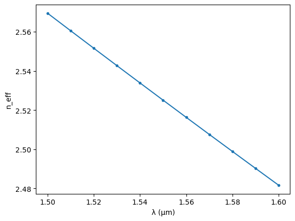
straight_neffs = waveguide_solver.n_eff[:, 0]
plt.plot(straight_wavelengths, straight_neffs.real, ".-")
plt.xlabel("λ (µm)")
plt.ylabel("n_eff")
plt.show()
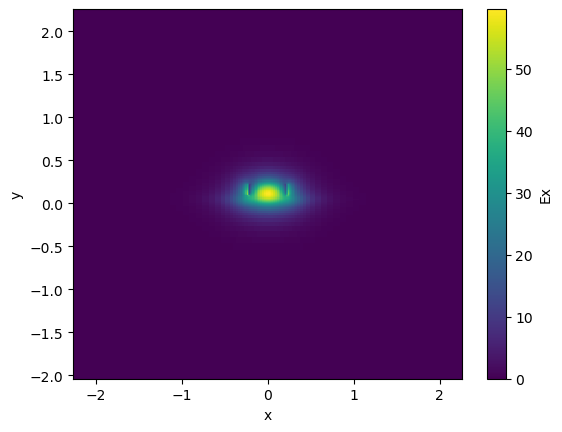
waveguide_solver.plot_field('Ex')
1
2
3
4
5
6
7
[32m2025-12-10 01:54:25.759[0m | [1mINFO [0m | [36mgplugins.tidy3d.modes[0m:[36m_data[0m:[36m266[0m - [1mload data from /home/ramprakash/.gdsfactory/modes/Waveguide_041c32d6f4a389a6.npz.[0m
/home/ramprakash/anaconda3/envs/si_photo/lib/python3.13/site-packages/numpy/_core/getlimits.py:559: UserWarning: The value of the smallest subnormal for <class 'numpy.float64'> type is zero.
setattr(self, word, getattr(machar, word).flat[0])
/home/ramprakash/anaconda3/envs/si_photo/lib/python3.13/site-packages/numpy/_core/getlimits.py:91: UserWarning: The value of the smallest subnormal for <class 'numpy.float64'> type is zero.
return self._float_to_str(self.smallest_subnormal)
1
<matplotlib.collections.QuadMesh at 0x7838c26f74d0>
Source Code
1
2
3
4
5
6
7
8
9
10
11
12
13
14
15
16
17
18
19
20
21
@jax.jit
def complex_interp(xs, x, y):
    ys_mag = jnp.interp(xs, x, jnp.abs(y))
    ys_phase = jnp.interp(xs, x, jnp.unwrap(jnp.angle(y)))
    return ys_mag * jnp.exp(1j * ys_phase)


@jax.jit
def straight_model(wl=np.linspace(1.45, 1.65, 50), length: float = 1.0):
    n_eff = complex_interp(wl, straight_wavelengths, straight_neffs.real)
    s21 = jnp.exp(2j * jnp.pi * n_eff * length / wl)
    zero = jnp.zeros_like(wl)
    return {
        ("o1", "o1"): zero,
        ("o1", "o2"): s21,
        ("o2", "o1"): s21,
        ("o2", "o2"): zero,
    }


straight_model(wl=1.55)
1
2
3
4
{('o1', 'o1'): Array(0., dtype=float64, weak_type=True),
 ('o1', 'o2'): Array(-0.68878147-0.72496902j, dtype=complex128),
 ('o2', 'o1'): Array(-0.68878147-0.72496902j, dtype=complex128),
 ('o2', 'o2'): Array(0., dtype=float64, weak_type=True)}
Compact model for the coupler region
Source Code
1
2
3
4
5
6
7
8
9
10
11
gap=0.2
length_x=0
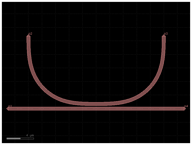
coupler_ring_par = partial(
gf.components.coupler_ring,
gap=gap,
length_x=length_x,
cross_section='strip'
)
coupler_ring = coupler_ring_par(gap=gap, length_x=length_x)
coupler_ring.draw_ports()
coupler_ring.plot()
Source Code
1
2
3
4
5
6
7
8
9
10
11
12
13
14
15
16
17
18
19
20
21
22
23
24
25
26
27
28
29
30
31
32
33
34
35
36
from pathlib import Path
wavelengths = np.linspace(1.5, 1.6, 50)
Si = mp.Medium(index=3.45)
SiO2 = mp.Medium(index=1.45)

resolution = 20
dpml = 1
pad = 1
s = gmeep.write_sparameters_meep_mpi(
        coupler_ring,
        cores=16,
        xmargin_left=1,
        xmargin_right=1,
        ymargin_top=1,
        ymargin_bot=1,
        port_source_names=['o1'],
        port_source_modes={'o1':[0]},
        port_modes=[0],
        filepath=Path(f'/home/ramprakash/Integrated_Tests/test_outputs/coupler_ring_gap_0.2.npz'),
        tpml=dpml,
        # extend_ports_length=0,  # Extend ports to create space for sources/monitors
        resolution=resolution,
        wavelength_start=wavelengths[0],
        wavelength_stop=wavelengths[-1],
        wavelength_points=len(wavelengths),
        port_source_offset=-0.5,
        port_monitor_offset=-0.1,
        distance_source_to_monitors=0.3,
        # port_symmetries=port_symmetries_coupler,
        layer_stack=layer_stack,
        # material_name_to_meep=dict(si=core_material),
        is_3d=False,
        overwrite=False,
        run=False
        )
1
[32m2025-12-10 01:55:04.996[0m | [1mINFO [0m | [36mgplugins.gmeep.write_sparameters_meep_mpi[0m:[36mwrite_sparameters_meep_mpi[0m:[36m148[0m - [1mSimulation PosixPath('/home/ramprakash/Integrated_Tests/test_outputs/coupler_ring_gap_0.2.npz') already exists[0m
Source Code
1
2
3
4
5
6
7
import gplugins
sp = np.load(s)
kappa = np.abs(sp["o3@0,o1@0"])
tau = np.abs(sp["o4@0,o1@0"])
plt.plot(wavelengths,kappa)
# plt.plot(wavelengths,tau)
# gplugins.plot.plot_sparameters(sp, logscale=True)
1
[<matplotlib.lines.Line2D at 0x7370e1ed4550>]
Source Code
1
2
3
4
5
6
7
8
9
10
11
12
13
14
15
16
17
18
19
20
21
22
23
24
25
26
27
28
29
30
31
32
33
34
35
36
37
38
39
40
41
42
43
44
45
46
47
48
49
50
51
52
53
54
55
56
57
58
59
60
61
62
63
64
65
66
def coupler_model(
    gap: float = 0.2,
    length_x: float = 1.0,
    cross_section: gf.typings.CrossSectionSpec = "strip",
    wavelengths: list =np.linspace(1.45, 1.65, 50)
):
    component = coupler_ring_par(
        gap=gap,
        length_x=length_x,
    )
    # separation = 2.0
    # bend_factor = 4.0
    resolution = 20
    dpml = 1
    pad = 1
    s = gmeep.write_sparameters_meep_mpi(
            component,
            cores=16,
            xmargin_left=1,
            xmargin_right=1,
            ymargin_top=1,
            ymargin_bot=1,
            port_source_names=['o1'],
            port_source_modes={'o1':[0]},
            port_modes=[0],
            filepath=Path(f'/home/ramprakash/Integrated_Tests/test_outputs/coupler_ring_gap_{gap}.npz'),
            tpml=dpml,
            # extend_ports_length=0,  # Extend ports to create space for sources/monitors
            resolution=resolution,
            wavelength_start=wavelengths[0],
            wavelength_stop=wavelengths[-1],
            wavelength_points=len(wavelengths),
            port_source_offset=-0.5,
            port_monitor_offset=-0.1,
            distance_source_to_monitors=0.3,
            # port_symmetries=port_symmetries_coupler,
            layer_stack=layer_stack,
            # material_name_to_meep=dict(si=core_material),
            is_3d=False,
            overwrite=False,
            run=False
            )

    # wavelengths = s.pop("wavelengths")

    @jax.jit
    def _model(wl=1.55):
        s11 = complex_interp(wl, wavelengths, np.load(s)["o1@0,o1@0"])
        s21 = complex_interp(wl, wavelengths, np.load(s)["o2@0,o1@0"])
        s31 = complex_interp(wl, wavelengths, np.load(s)["o3@0,o1@0"])
        s41 = complex_interp(wl, wavelengths, np.load(s)["o4@0,o1@0"])
        return sax.reciprocal({
            ("o1", "o1"): s11, # reflection
            ("o1", "o2"): s21, # isolation
            ("o1", "o3"): s31, # coupling
            ("o1", "o4"): s41, # through
        })

    return _model


coupler_model(
    gap=gap,
    length_x=length_x,
    wavelengths=wavelengths
)()
1
2
3
4
5
6
7
8
9
10
11
12
13
[32m2025-12-10 02:12:57.412[0m | [1mINFO [0m | [36mgplugins.gmeep.write_sparameters_meep_mpi[0m:[36mwrite_sparameters_meep_mpi[0m:[36m148[0m - [1mSimulation PosixPath('/home/ramprakash/Integrated_Tests/test_outputs/coupler_ring_gap_0.2.npz') already exists[0m
{('o1', 'o1'): Array(-0.03180084-8.44300366e-05j, dtype=complex128),
('o1', 'o2'): Array(-0.00107009+0.00051673j, dtype=complex128),
('o1', 'o3'): Array(-0.14948838+0.06935893j, dtype=complex128),
('o1', 'o4'): Array(0.8009763+0.57550373j, dtype=complex128),
('o2', 'o1'): Array(-0.00107009+0.00051673j, dtype=complex128),
('o3', 'o1'): Array(-0.14948838+0.06935893j, dtype=complex128),
('o4', 'o1'): Array(0.8009763+0.57550373j, dtype=complex128)}
Building the Ring modulator circuit
NOTE: Here the circuit is build using the ideal coupler and also the whole is considered to be the doped region. Also there since the doped region is considered as straight no bend losses is taken to account. So take the results with a huge grain of salt
FIX: Add the bend losses. Propper coupler design instead of ideal coupler.
Source Code
1
2
3
4
5
6
7
8
9
10
11
12
13
14
15
16
17
18
19
20
21
22
23
24
25
26
27
# Use this to load the model without errors
def coupler_model(wl=1.55, gap=0.2, length_x=0.0):
    """
    Returns S-parameters directly (no inner function)
    """
    # Load data
    sparam_file = Path(f'test_outputs/coupler_ring_gap_{gap}.npz')
    sp_data = np.load(sparam_file, allow_pickle=True)
    wavelengths = sp_data['wavelengths']

    # Interpolate
    s11 = complex_interp(wl, wavelengths, sp_data["o1@0,o1@0"])
    s21 = complex_interp(wl, wavelengths, sp_data["o2@0,o1@0"])
    s31 = complex_interp(wl, wavelengths, sp_data["o3@0,o1@0"])
    s41 = complex_interp(wl, wavelengths, sp_data["o4@0,o1@0"])

    # Return S-parameters DIRECTLY (no @jax.jit, no inner function)
    return sax.reciprocal({
        ("o1", "o1"): s11,
        ("o1", "o2"): s21,
        ("o1", "o3"): s31,
        ("o1", "o4"): s41,
    })

# This should return S-parameters, not a function
sp = coupler_model(wl=1.55, gap=0.2)
sp
1
2
3
4
5
6
7
{('o1', 'o1'): Array(-0.03180084-8.44300366e-05j, dtype=complex128),
 ('o1', 'o2'): Array(-0.00107009+0.00051673j, dtype=complex128),
 ('o1', 'o3'): Array(-0.14948838+0.06935893j, dtype=complex128),
 ('o1', 'o4'): Array(0.8009763+0.57550373j, dtype=complex128),
 ('o2', 'o1'): Array(-0.00107009+0.00051673j, dtype=complex128),
 ('o3', 'o1'): Array(-0.14948838+0.06935893j, dtype=complex128),
 ('o4', 'o1'): Array(0.8009763+0.57550373j, dtype=complex128)}
Source Code
1
2
3
4
5
import gdsfactory as gf
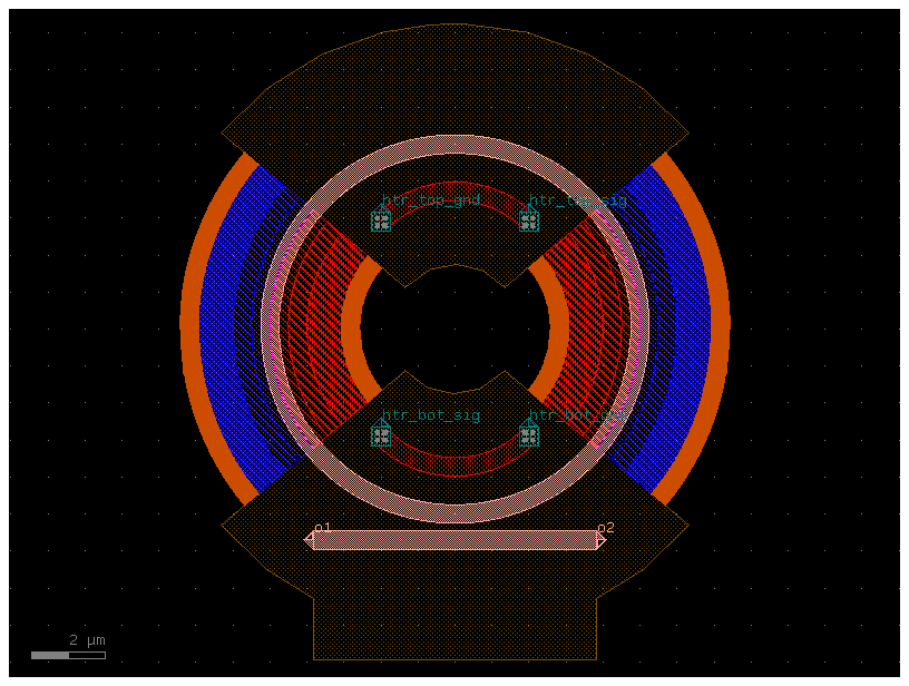
c = gf.components.ring_double_pn(add_gap=0.2, drop_gap=0.2, radius=5, doping_angle=80, doped_heater=True, doped_heater_angle_buffer=10, doped_heater_layer='NPP', doped_heater_width=0.5, doped_heater_waveguide_offset=2.175, with_drop=False)
c.draw_ports()
c.plot()
Source Code
1
2
3
4
5
6
7
8
9
10
11
12
13
14
15
16
17
18
19
20
21
22
23
24
25
26
27
28
29
30
31
32
33
34
35
# netlist={
#     "instances":{
#         "coupler_bus":"coupler",
#         "bus_wg":"straight",
#         "through_wg":"straight",
#         "passive_wg":"straight",
#         "active_wg":"active",
#     },
#     "connections":{
#         "bus_wg,o2":"coupler_bus,o1",
#         # "coupler_bus,o1":"coupler_bus,o3",
#         "coupler_bus,o3":"active_wg,o1",
#         "active_wg,o2":"coupler_bus,o2",
#         # "passive_wg,o2":"coupler_bus,o2",
#         "coupler_bus,o4":"through_wg,o1"

#         # "coupler_bus,o3":"active_wg,o1",
#         # "active_wg,o2":"passive_wg,o1",
#         # "passive_wg,o2":"coupler_bus,o2",
#         # "coupler_bus,o4":"through_wg,o1"
#     },
#     "ports":{
#         "in":"bus_wg,o1",
#         "out":"through_wg,o2",
#         # "in":"coupler_bus,o1",
#         # "out":"coupler_bus,o4",
#     },
# }
# models={
#     "active":phase_shifter_pn_junction,
#     "straight":straight_model,
#     "coupler":coupler_model
# }

# ring, info = sax.circuit(netlist=netlist, models=models)
Source Code
1
2
3
4
5
6
7
8
9
10
11
12
13
14
# # Ring paramters
# R = 30 # radiums
# L = 2*np.pi*R
# La = 0 # active length
# Lp = L

# wl = jnp.linspace(1.5, 1.6, 1000)
# S = ring(wl=wl, passive_wg={"length": 0}, active_wg={"length": L, })

# plt.plot(wl * 1e3, abs(S["in", "out"]) ** 2)
# plt.ylim(-0.05, 1.05)
# plt.xlabel("λ [nm]")
# plt.ylabel("T")
# plt.show()
Source Code
1
2
3
4
5
6
7
8
9
10
11
12
13
14
15
16
17
18
19
20
21
22
23
24
25
26
27
28
29
30
31
32
33
34
35
ring_length = 100.0  # [μm] Length of the ring
coupling = 0.5  # [] coupling of the coupler
wl = jnp.linspace(1.5, 1.6, 1000)  # [μm] Wavelengths to sweep over
voltage=5
_all_pass_sax, _ = sax.circuit(
    netlist={
        "instances": {
            "dc": {"component": "coupler", "settings": {"coupling": coupling}},
            "active": {
                "component": "straight",
                "settings": {
                    "length": ring_length,
                    "voltage": voltage,
                },
            },
        },
        "connections": {
            "dc,out1": "active,o1",
            "active,o2": "dc,in1",
        },
        "ports": {
            "in0": "dc,in0",
            "out0": "dc,out0",
        },
    },
    models={
        "coupler": sax.models.coupler_ideal,
        "straight": phase_shifter_pn_junction,
    },
)


def all_pass_sax(wl=1.5, voltage=50):
    sdict = sax.sdict(_all_pass_sax(wl=wl, voltage=voltage))
    return abs(sdict["in0", "out0"]) ** 2
Source Code
1
2
3
4
5
6
7
8
9
# fig, ax = plt.figure()
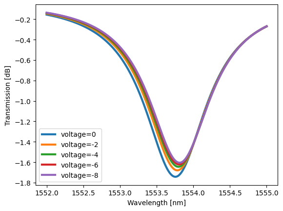
wl = jnp.linspace(1.552, 1.555, 1000)
for voltage in np.arange(0, -10, -2):
detected_sax = all_pass_sax(wl=wl, voltage=voltage) # non-jitted evaluation time
plt.plot(wl * 1e3, 20*np.log10(detected_sax), label=f"voltage={voltage}", lw=3)
plt.legend()
plt.xlabel("Wavelength [nm]")
plt.ylabel("Transmission [dB]")
plt.show()